
Trenz Electronic System-on-Modules (SoMs)
19 Mar 2024 - 19 Mar 2024
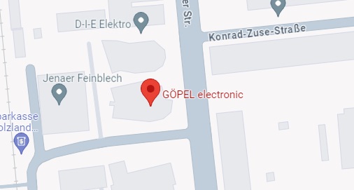
Germany, Jena
Powered by MPS
In this workshop, we offer a comprehensive introduction to the integration of Trenz Electronic System-on-Modules (SoMs) using an AMD Xilinx System-on-Chip (SoC) for application in customer projects with custom carrier board.
We start with the criteria for selecting suitable SoMs and then focus on all the design steps involved in developing and bringing up such a custom carrier board.
This includes addressing both hardware and software aspects and providing an overview of all the necessary design steps: hardware design (Altium), software design (Vivado + Petalinux), and debugging techniques (Vivado).
The goal of the workshop is to provide the necessary overview to navigate the integration process, avoid common pitfalls, and develop successful SoM-based solutions.
Partners

Location
Göpel Electronic GmbH
Göschwitzer Str. 58/60
07745 Jena Germany
Agenda
| Date & Time | Session | |
|---|---|---|
| 09:00 - 09:30 | Introduction | |
| 9:30 - 11:30 | Hardware (Trenz Electronic) | |
| 11:30 - 12:30 | Software Part 1 (Trenz Electronic) | |
| 12:30 – 13:30 | Lunch | |
| 13:30 - 14:30 | Software Part 2 (Trenz Electronic) | |
| 14:30 – 15:30 | Debugging (Avnet Silica) | |
| 15:30 – 16:30 | The ideal Power supplier for AMD / Trenz FPGA SoM will present suitable solutions (MPS) | |
| 16:30 | End | |
Registration
Registration is closed.
Topics
Hardware
- Selecting a Trenz module
- Interfaces, periphery
- FPGA/SoC
- Resources
- Power requirements
- Series and variants
- Customization
- Upgrade ability
- Trenz carrier
- Get ready for prototyping
- Limitations
- Custom carrier design
- Module HW configuration
- IO planning / MIO setup
(Software excursion) - Gain compatibility
- IO planning / MIO setup
- Power sequencing
- Length matching
- Thermal management
- Pitfalls
- Module HW configuration
- Custom module / Chip-down (NRE)
Software
- Initial Setup with Trenz-Carrier and Reference Design
- Introduction via Public Doc --> hands on Trenz Wiki / Docu
- Board Variants
- Possible Flows / Scripting
- Boot Options Support
- Initial Verification of custom PS/PL
- IO Planning / MIO Setup / Constraints Check (will be done earlier)
- From Reference Design to "Individual Test Design with examples"
- Adding periphery (PS/EMIO/IP)
- I2C
- SPI
- Prop rietary
- GTs
- Testing strategy
- Automation for Tests
- Adding periphery (PS/EMIO/IP)
Debug
After the design phase of an FPGA board has been completed, it is typically time for bringing up and testing of the board. For this step it is good to have powerful debugging tools available.
AMD offers the following tools, which we will briefly examine in detail:
- ILA / System ILA
The Integrated Logic Analyzer offers the possibility to record signals and interfaces in the FPGA in real time. The tool has many features that are known from discrete logic analyzers. - VIO
With the Virtual Input/Output unit, stimuli can easily be brought into the design and individual signals of the design can be displayed. You can think of this function as virtual DIP-Switches and LEDs. - JTAG to AXI
A master functionality that allows access to AXI interfaces via TCL script and JTAG. Read/ write and burst accesses are thus possible without own software in the FPGA. - xsct Console
This console accesses a processor system in the FPGA via JTAG and offers functions such as register dump, read/write memory areas, singlestep and much more. - Add Probe
Offers the possibility to route single signals from a routed design to free pins of the FPGA. The existing design is not changed and the FPGA can be accessed with external measuring equipment. - Traffic Generator / Performance Monitor
In designs with many AXI interfaces, it is often not easy to find out whether the desired performance is still given. Bottlenecks can be identified very elegantly with the Traffic Generator / Performance Monitor.